- Slow positron beam
- Coincidence Doppler broadening
- Fast positron spectrometers
Slow positron beam
Slow positron measurements are performed by moderating positrons emitted by an 50 mCi (year 2021) sealed radioactive source and then implanting them into the sample with a kinetic energy ranging from few eV to 20 keV. The positron implantation depth is a few microns, depending on the sample density.

Reasons for using a beam
The high sensitivity of positrons to open surface defects makes desirable using Positron Annihilation Spectroscopy (PAS) for studying the defect strucure of thin films and sub-surface layers. This is impossible with e+ directly coming from a radioactive source of 22Na, since they are very fast (kinetic energy up to 0.54 MeV) and are implanted very deeply (tens of microns) into the sample. The chance of annihilation near to the free surface or even emission as positronoum (Ps) from the surface is practically null. The remedy is to use a monoenergetic beam, tunable from 0.1 keV up to 20 keV. This allows one to explore selectively subsurface layers from a few tens of nanometres up to a micrometric depth (depending on the density of the studied material, approximately one micrometer in Si). The depth resolution is limited by the width of the implantation profile and by the diffusion of the positrons after thermalisation. Most positrons implanted at less than about tens of nanometers may return to the surface by diffusion and be emitted as bare positrons or as Ps. This is interesting for obtaining Ps in vacuum.
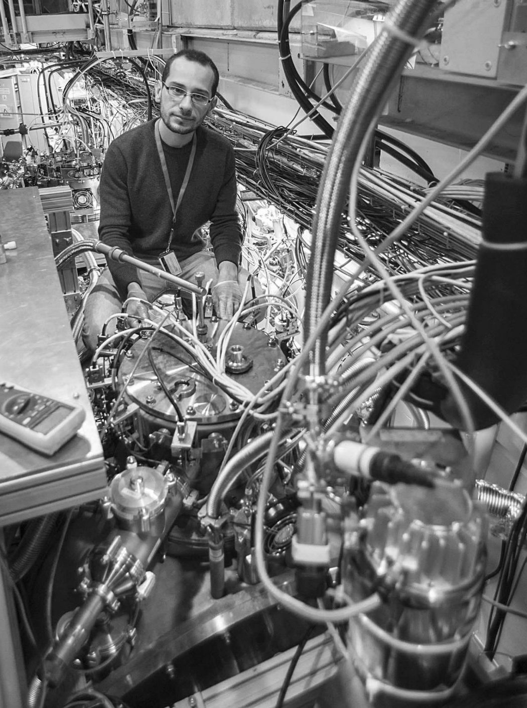
The L-NESS beam

The beam is operative in our lab since 2010. It gives a continuous positron current at the sample 105 e+/s (with 50 mCi in 2021) on a spot of about 2 mm FWHM, with energy tunable from 0.1 to 20 keV. It is a fully electrostatic system, comprised of the following parts: a) Primary radioactive source (about 50 mCi of 22Na, in 2021); b) Moderator (W [100], 1 micrometer thick), where a small fraction (about 10-3) of the positron flux thermalises and is emitted from the surface at the energy corresponding to the negative workfunction of the positrons in W (at about 2.5 eV); c) electron optics for transport of fixed energy (1 keV); d) energy filtering by beam bending (suppression of the high energy background); d) electron optics for energy tuning and final focusing. Automatic energy scan is implemented.

Slow positron beam. 1. Radioactive source; 2. Electrostatic optics; 3. Sample chamber; 4. HpGe detectors; 5. Cryostat; 6. High voltage protection cage; 7. Power suppliers; 8. Detector electronics.
The positron beam is equipped with HpGe detectors for momentum distribution measurements, which can be operated in both single and coincidence mode. Samples are kept in high vacuum (10-6-10-8 mbar, depending of the studied problem) and their temperature can be varied from 10 to 1100 K. The slow positron beam has been calibrated for positronium fraction measurements.
Depth Profile

Makhov profile showing the implantation profile as a function of positron energy in Si. The dashed lines correspond to the mean penetration depth z.
Coincidence Doppler Broadening

( after Asoka-Kumar et al. Phys. Rev. Lett.77 (1996) 2097)
What is Coincidence Doppler broadening? CDB is the one technique developed by Kelvin Lynn and collaborators [3,4] giving information on the chemical composition of solute aggregates containing open volume defects (vacancies or misfit regions). This is a very important information, since vacancies help the transport of the solute in the solid matrix and affect the stability of the aggregates by relieving the local stress due to different atomic sizes. The method for obtaining the full quantitative analysis has been proposed and improved by our group.

Block diagram of the CDB system.

This is the bi-dimensional energy spectrum of annihilation photon pairs. The diagonal marked with red arrows corresponding to energy conservation (2m0c2). The central peak is elongated along the diagonal due to the Doppler effect.
This is the momentum spectrum obtained by cutting the bi-dimensional energy spectrum along the diagonal (red arrows). The high-momentum tails are due to annihilations with fast core electrons and carry information on the atomic species. It is possible to obtain the S and W parameters to characterize the annihilation peak. The Positron Laboratory is equipped with a CDB spectrometer.

The high-momentum details are enhanced when shown in terms of relative difference to a reference spectrum. The spectrum for an Al-Zn-Mg-Cu alloy as-quenched (open symbols green, left side frame) is reproduced by a linear combination (dashed green line) of the spectra measured for pure metals saturated of defects (right-side frame). For more details see Refs. 5 and 6 (and references therein).
CDB is performed by means of two HpGe detectors with an energy resolution of about 1.2 keV on the annihilation line. The two detectors are coupled with a multi-parametric pulse analyzer which allows for coincidence measurements at a very high signal to noise ratio. Samples can be measured at temperature in a range between 10 to 1100 K (in the positron beam) and with fast positrons between 10 and 500 K.
Fast positron lifetime spectrometers

Positron lifetime spectrometer. 1. Scintillators and photomultipliers; 2. Sample; 3. Liquid nitrogen Dewar; 4. Detector electronics.
Fast positrons are obtained by the radioactive decay of a 22Na sealed radioactive source sandwiched between two identical samples. Positrons are emitted from the source with an high energy (22Na has a positron endpoint energy of 540 keV) and sampled several hundred microns from the surface of the specimen.
Our laboratory is equipped with two analog gamma ray spectrometers for PL measurements with a time resolution of about 250 ps. The gamma spectrometers are fast scintillators (BaF and plastic scintillators) coupled with photomultipliers.
Samples can be measured at temperature in a range between with fast positrons between 10 and 500 K.
References
[1] R. Ferragut, A. Calloni, A. Dupasquier, G. Isella: Defect characterization in SiGe/SOI epitaxial semiconductors by positron annihilation. Nanoscale Res. Lett. 5, 1942 (2010)
[2] A. Calloni, R. Ferragut, F. Moia, A. Dupasquier, G. Isella, D. Marongiu, G. Norga, A. Federov, and D. Chrastina: Positron annihilation studies of defects in Si1-xGex/SOI heterostructures, phys. stat. sol. (c) 6, 2304 (2009)
[3] J. R. MacDonald, R. A. Boie, L. C. Feldman, M. F. Robbins, P. Mauger and K. G. Lynn, Bull. Am. Phys. Soc. 24 580 (1975)
[4] K. G. Lynn, J. R. MacDonald, R. A. Boie, L. C. Feldman, J. D. Gable and M. F. Robbins, Phys. Rev. Lett. 38 241 (1977)
[5] A. Dupasquier, R. Ferragut, M. M. Iglesias, M. Massazza, G. Riontino, P. Mengucci, G. Barucca, C. E. Macchi, and A. Somoza, Phil. Mag. 87 3297 (2007)
[6] R. Ferragut, A. Dupasquier, C. E. Macchi, A. Somoza, R. N. Lumley, and I. J. Polmear, Scripta Mater. 60 137 (2009)